
Semiconductor Innovations on TSMC s N3P Node
The N3P node represents a practical kind of progress in advanced chipmaking: not a dramatic reset, but a refined step that gives designers more room to improve performance, power, and density. For companies building premium mobile processors, AI accelerators, and high-performance computing silicon, that kind of refinement can be just as important as a brand-new architecture. It also shows where the future of semiconductors is heading: toward tighter collaboration between process technology, lithography, packaging, design tools, and talent development.
Why does N3P matter for advanced semiconductors?
N3P matters because it extends the value of TSMC’s 3nm family while giving chip designers a more optimized path beyond N3E. TSMC describes N3P as an optical shrink of N3E that improves performance, reduces power, increases transistor density, and remains compatible with N3E design rules, which can help teams reuse more design work instead of starting from scratch.
That balance is central to modern semiconductor innovations. The most advanced semiconductors are no longer judged only by whether a node is smaller. They are judged by whether the node helps a real product ship with better battery life, higher sustained performance, lower heat, improved area efficiency, or a more manageable development cycle.
N3P sits in that useful middle ground. It does not replace the excitement around nanosheet transistors, backside power delivery, or future angstrom-class roadmaps. Instead, it strengthens a proven FinFET platform at a time when AI workloads, mobile devices, and high-performance computing products all need more efficient silicon.
What changes from N3E to N3P?
The simplest answer is that N3P refines N3E rather than reinventing it. Public reporting based on TSMC disclosures has described N3P as offering roughly a 4% to 5% performance uplift or a meaningful power reduction versus N3E, along with about a 4% density improvement for a mixed chip design, while preserving N3E design-rule compatibility.
Those numbers may look modest compared with older “full-node” leaps, but they are valuable in today’s design environment. At leading edge nodes, every percent matters because designers are fighting limits in power delivery, thermal behavior, SRAM scaling, analog integration, verification time, and cost. A small improvement at the process level can become a noticeable product advantage when paired with smarter architecture, better software scheduling, and advanced packaging.
Key N3P implications include:
- More efficient performance tuning: Designers can target higher frequency at similar leakage or prioritize lower power at similar clocks, depending on the product.
- Better density without a major reset: An optical shrink can help improve area efficiency while keeping continuity with the N3E ecosystem.
- Lower migration friction: Compatibility with N3E design rules can make N3P more attractive for teams already working within the N3 family.
- A longer runway for FinFET designs: N3P helps keep advanced FinFET technology relevant even as TSMC moves into nanosheet-based N2 and beyond.
This is why semiconductor advancements often arrive as families rather than single nodes. N3, N3E, N3P, and N3X are not merely labels. They reflect different tradeoffs for smartphones, AI chips, high-performance CPUs, and other products that do not all need the same mix of speed, leakage, area, and cost.
Semiconductor innovation is becoming a system-level discipline
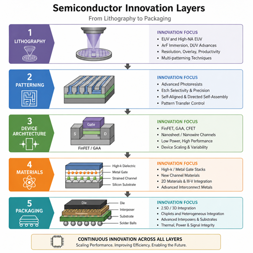
The story of N3P is not only about transistor scaling. It is part of a larger shift in semiconductor research, where improvements come from the interaction of process technology, lithography, design-technology co-optimization, packaging, and software-aware architecture.
TSMC’s broader roadmap makes that direction clear. The company has positioned its 3nm family as advanced FinFET technology, while its newer N2 platform moves to nanosheet transistors, and its A16 technology combines nanosheet transistors with a backside power rail architecture for planned production in 2026.
That roadmap matters because chip progress is now constrained by more than transistor count. As interconnects become harder to scale, power delivery becomes more complex, and AI models push compute demand upward, the industry needs improvements at every layer. Semiconductor industry innovations increasingly depend on how well these layers work together.
Lithography remains at the center
Advanced lithography is still one of the foundations of leading-edge manufacturing. ASML has stated that AI adoption is expanding across applications and that the industry will need major innovations to address AI power consumption and cost challenges; it also expects lithography to remain central to customer innovation.
For nodes like N3P, lithography improvements are not abstract. Pattern fidelity, overlay control, process windows, and exposure strategy all influence how consistently dense features can be printed at scale. Even when a node is described as an optical shrink, that phrase points to an ecosystem of scanners, process control, masks, computational lithography, metrology, and manufacturing learning.
Packaging is part of the node conversation
The most advanced chips are also increasingly limited by how they move data and power across a system. TSMC has highlighted CoWoS, SoIC, and system-level integration as part of its AI technology portfolio, noting that CoWoS allows customers to place processor cores and high-bandwidth memory stacks side by side on an interposer.
That matters for N3P because a leading-edge die rarely succeeds alone. A powerful accelerator may need high-bandwidth memory, advanced substrates, chiplet interconnects, and thermal design choices that let the silicon operate efficiently. The node supplies one part of the advantage; packaging determines how much of that advantage the final system can actually use.
Practical design choices become more important on N3P
For chip teams, N3P is not simply a “better N3E.” It is a set of options. The best use of the node depends on product goals, workload behavior, and the maturity of the design organization.
A mobile system-on-chip might use N3P to reduce power during everyday workloads, extending battery life or creating more thermal headroom for camera, AI, and graphics features. A data center accelerator might use the gain differently, prioritizing sustained throughput within a strict power envelope. A high-performance CPU could combine process gains with microarchitectural tuning to improve peak and sustained frequency.
A practical N3P evaluation checklist should include:
- Workload priority: Decide whether the product needs burst performance, sustained efficiency, area savings, or a blend of all three.
- IP readiness: Review which existing N3E IP can migrate cleanly and which blocks need extra validation.
- Power delivery strategy: Model voltage, current density, thermal hotspots, and package-level constraints early.
- SRAM and analog balance: Consider whether the design is logic-heavy, memory-heavy, analog-heavy, or mixed, because density benefits vary by block type.
- Packaging plan: Match the node decision with memory bandwidth, interconnect, substrate, and cooling assumptions.
- Software behavior: Profile real workloads so silicon improvements are not wasted by inefficient scheduling or memory movement.
This is where semiconductor research turns into product strategy. A node can provide better raw capability, but product teams still need to decide where to spend that capability. The winning design is rarely the one that chases every benchmark at once. It is the one that aligns silicon, packaging, firmware, and user value.
AI is raising the stakes for efficiency
AI is one of the strongest forces shaping semiconductor advancements because it changes both compute demand and design priorities. Training and inference workloads require massive parallelism, fast memory movement, and predictable power behavior. That pressure reaches from cloud accelerators down to edge devices and smartphones.
N3P is relevant because it helps address the near-term efficiency problem while the industry prepares for larger architectural shifts. Not every product can wait for a later nanosheet node, and not every design needs the risk or cost profile of the newest option. A refined 3nm-class process can be the right choice when the product needs leading-edge performance with a more evolutionary design path.
The future of semiconductors will likely include more specialized engines, more chiplets, more advanced packaging, and more careful workload partitioning. But those trends do not reduce the importance of process nodes. They make the node one part of a more complex optimization problem.
Talent and education are part of semiconductor innovation
The conversation around N3P naturally leads to engineering talent. Advanced semiconductors require specialists in device physics, lithography, EDA, packaging, materials, reliability, software, and manufacturing operations. Without a strong talent pipeline, even the best roadmap becomes harder to execute.
That is why terms like “ASML semiconductor education innovations 2026” are more than search phrases. They point to a real industry need: inspiring and preparing the next generation of engineers. ASML’s education initiatives include STEM programs, employee involvement in classrooms, and the ASML Junior Academy, which the company says aims to reach 190,000 children in the coming years.
In the United States, The Tech Interactive announced a three-year, $1.65 million ASML grant in May 2026 to expand access to hands-on STEM experiences, including support for Title I field trips, The Tech Challenge, and career pathway exposure.
These efforts may seem far from a 3nm process node, but they are connected. Semiconductor industry innovations depend on long-term curiosity, training, and cross-disciplinary collaboration. The engineer who improves overlay control, the researcher who studies new materials, and the student who first discovers chip design through a hands-on STEM program are all part of the same innovation pipeline.
What does N3P tell us about the future of semiconductors?
N3P shows that the future of semiconductors will be built through both breakthrough technologies and disciplined refinements. The industry still needs major transitions, such as nanosheet transistors, backside power delivery, and more advanced 3D integration, but it also needs mature, manufacturable improvements that help products ship sooner and perform better.
That lesson is important for anyone tracking semiconductor innovations. Progress is not always dramatic from the outside. Sometimes it appears as a few percentage points of performance, a cleaner migration path, a denser layout, a better package, or a more capable design ecosystem. At scale, those details can influence millions of devices and enormous compute infrastructure.
TSMC’s roadmap illustrates this layered future. N3P strengthens the 3nm family, N2 introduces nanosheet transistor technology, and A16 adds backside power rail concepts for future high-performance products. Meanwhile, ASML’s ecosystem work, including collaborative research into 3nm semiconductor technology through the PIn3S pilot project, reflects how much innovation now depends on partnerships across companies, suppliers, institutes, and governments.
Key takeaways for industry watchers
N3P is best understood as an enabling node, not just a process update. It gives designers more flexibility within the 3nm family and reinforces several broader trends shaping semiconductor research.
Important takeaways include:
- Refinement is innovation: Smaller node updates can still produce meaningful gains when applied to real products.
- Compatibility has strategic value: Reusing parts of the N3E design ecosystem can reduce friction for teams moving to N3P.
- Efficiency is the main battlefield: AI, mobile, and data center workloads all make power and thermal behavior central design concerns.
- Packaging and lithography are inseparable from scaling: The value of a node depends on manufacturing precision and system integration.
- Education is part of the roadmap: Future semiconductor advancements require a workforce that understands both deep physics and system-level design.
N3P captures the current moment in chipmaking well. The industry is still scaling, but it is scaling more carefully, with more attention to tradeoffs and more dependence on ecosystem coordination.
A grounded step toward the next era
TSMC’s N3P node is not the final destination for advanced semiconductors. It is a smart, practical step in a longer journey toward nanosheet devices, backside power delivery, denser packaging, and more specialized computing architectures. Its importance comes from how it bridges today’s production realities with tomorrow’s technology ambitions.
For designers, N3P offers another way to tune performance, power, and density inside a familiar 3nm framework. For the broader industry, it shows that semiconductor innovations are becoming more integrated, more collaborative, and more system-aware. That is the real story: the future of semiconductors will be shaped not by one breakthrough alone, but by many connected advancements working together.