
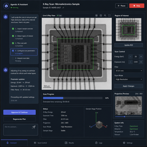
Agentic AI is beginning to change how researchers inspect the tiny structures inside microelectronics. Instead of manually steering every X-ray scan, scientists can describe what they want in everyday language, while an AI-enabled system helps find regions of interest, process images, and recommend the next experimental step. For advanced microelectronics, this points toward faster, more adaptive inspection workflows that keep humans in control while reducing repetitive instrument work.
What does agentic AI change about X-ray microelectronics research?
Agentic AI changes X-ray microelectronics research by moving AI from a passive analysis tool to an active experimental assistant. In a recent Argonne National Laboratory demonstration within the Synergistic Neutron and Photon Science—Intelligence project, researchers showed a system that can translate natural-language instructions into beamline actions, process data, analyze images, and decide when to ask for human guidance. That makes agentic ai x-ray microelectronics more than a keyword; it describes a practical shift toward self-guided scientific instrumentation.
Traditional X-ray experiments at advanced facilities often require highly trained operators to manage scan setup, region selection, data reconstruction, and follow-up imaging. Those steps are powerful, but they can be slow when a sample is complex or when the feature of interest is hard to define in advance. Agentic AI adds a planning layer: the system can observe what a scan reveals, choose a sensible next move, and adapt its path rather than simply running a fixed script.
This does not mean scientists disappear from the process. The more realistic near-term model is human-in-the-loop autonomy, where the AI performs lower-risk actions on its own and pauses for approval when uncertainty or risk rises. That balance matters in microelectronics technology, where a tiny defect, interface, or material transition can carry major implications for performance, reliability, and future device design.
From natural language to self-guided scans
The most accessible part of this development is the interface. A researcher can make a plain-language request such as measuring a region or mapping an area at higher resolution, rather than manually navigating every technical control. According to Argonne’s report, the demonstrated system uses those instructions to guide data collection and analysis, helping identify important features and recommend areas for closer inspection.
Behind that simple interaction is a layered workflow. The agent must understand the instruction, connect it to available instrument tools, collect an image, interpret the result, decide what should happen next, and then either act or ask for confirmation. In the Argonne demonstration, this included real-time image interpretation with a ptychographic model called PtychoFM and vision capabilities from a multimodal large language model.
That is why the phrase “self-guided” is important. The AI is not merely labeling an image after the experiment ends. It is helping shape the experiment while it is running, which can make high-value facility time more productive and can reduce the burden of repetitive search tasks.
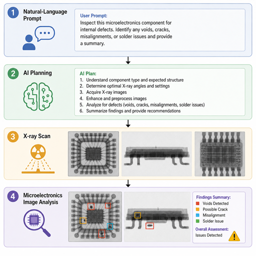
A simplified workflow looks like this:
- The scientist states the goal. The prompt might describe a sample area, a target feature, or a desired scan resolution.
- The agent plans the next action. It connects the request to instrument capabilities and available analysis tools.
- The system collects data. The beamline captures an image or scan from the selected region.
- AI interprets the result. Reconstruction, segmentation, or feature detection helps the agent understand what it is seeing.
- The agent adapts. It may move to a new area, refine the scan, switch to higher resolution, or ask the scientist for approval.
For researchers, the benefit is not simply convenience. It is the ability to handle uncertainty more gracefully. A microelectronics sample may include irregular features that cannot be reduced to a neat rule, and an agentic workflow can respond to what is actually present.
Why microelectronics is a natural fit
Microelectronics inspection is full of search problems. Researchers and engineers often need to locate small features within large, layered, or visually complex samples. In advanced microelectronics, the feature that matters may be a narrow interface, a subtle defect, an unexpected material distribution, or a structural change that only becomes obvious at the right scale.
That makes the field a strong candidate for autonomous AI systems. Fixed automation works well when the task is predictable, but region-of-interest discovery is often messy. Argonne’s team specifically highlighted region-of-interest searching as difficult to express in code because features can vary widely from sample to sample. The demonstrated agent addressed this by collecting an image, examining it, deciding where to move next, refining the search, and ultimately finding the target region.
The same pattern has broader relevance to smart electronics. As devices become more compact, integrated, and material-rich, inspection must keep pace with complexity. AI circuit design can help engineers explore architectures and optimize layouts, but physical characterization remains essential because manufactured structures do not always behave exactly like models. Agentic AI can help connect those worlds by making it easier to inspect real samples and feed insights back into design and process decisions.
The technology stack behind the experiment
Agentic AI sounds conversational on the surface, but its value comes from tool use. The system needs access to instruments, imaging models, data pipelines, and safety constraints. In the SYNAPS-I work, the effort connects neutron, X-ray, and microscopy experiments across national laboratories, with Argonne’s demonstration involving the Advanced Photon Source, the Argonne Leadership Computing Facility, and the Center for Nanoscale Materials.
Several components matter:
- Natural-language control: Scientists can communicate intent without writing low-level commands for every action.
- Real-time reconstruction: Imaging models help turn raw experimental data into interpretable images quickly enough to guide the next step.
- Multimodal reasoning: The agent uses both language and visual information, which is essential when decisions depend on what appears in an image.
- Segmentation tools: Argonne reported connecting the agent to Meta’s Segment Anything Model 3 so features could be isolated and labeled within images.
- Human approval gates: The system can act autonomously for lower-risk steps while escalating higher-risk or uncertain decisions.
This stack is one reason agentic AI differs from a conventional chatbot. A chatbot may answer questions; an agent can plan, call tools, evaluate outputs, and iterate. In a scientific facility, that difference is the bridge between “tell me what this image means” and “help me run the next scan intelligently.”
How close are we to autonomous AI-driven laboratories?
Autonomous AI-driven laboratories are becoming more realistic, but they are not the same as fully unsupervised science. Current demonstrations point toward controlled autonomy: AI can manage repetitive or well-bounded tasks, while scientists set goals, validate decisions, and handle scientific judgment. The Argonne work is described as a step toward self-driving microscopes, closed-loop experimentation, and automated defect-detection tools, not as a replacement for researchers.
Other research supports the same direction. A Nature Machine Intelligence paper published in 2026 described an agentic AI X-ray scientist that used structured tool access to align samples on a synchrotron beamline, plan actions, interpret observations, and adapt to unexpected experimental conditions. This is important because real scientific instruments are not tidy software demos; they involve noise, hardware limits, ambiguous results, and changing conditions.
For microelectronics, the likely path is incremental adoption. First, agentic AI helps with scan setup, navigation, and image triage. Then it supports closed-loop experiments where scan results automatically influence the next measurement. Over time, these systems may become routine assistants for materials characterization, semiconductor research, and quality-focused analysis.
Practical implications for engineers and researchers
The immediate value of agentic ai x-ray microelectronics is better use of expert attention. Scientists spend less time repeating instrument steps and more time deciding which questions matter. Beamline operators can focus on experimental quality, while the AI handles structured search and routine interpretation.
For teams working on microelectronics technology, the implications include:
- Faster feature discovery: AI-guided region searches can reduce the manual burden of finding small or irregular structures.
- More adaptive characterization: Scans can change direction based on what earlier scans reveal.
- Improved data flow: Automated reconstruction and segmentation can make results easier to review during the experiment.
- Stronger links between design and inspection: Findings from physical samples can inform future AI circuit design choices and process adjustments.
- More accessible advanced tools: Natural-language control may help more researchers work productively with complex instruments, although expert oversight remains essential.
The key is to treat agentic AI as an augmentation layer. It can accelerate decisions, but it still needs clear goals, validated tools, careful permissions, and domain expertise. In high-stakes research, autonomy without accountability is not a feature.
The road ahead for agentic AI in advanced microelectronics
The future of this field will depend on reliability, integration, and trust. Researchers need agents that can explain why they chose a region, record what actions they took, respect instrument limits, and make uncertainty visible. They also need systems that work across different samples, modalities, and facilities without requiring every workflow to be rebuilt from scratch.
If those challenges are met, agentic AI could become a standard layer in advanced microelectronics research. It may help scientists inspect complex devices, compare material behavior across scales, and detect subtle features that would otherwise require long manual searches. More importantly, it can make experimental work more responsive: each measurement can guide the next one.
The larger story is not that AI is taking over X-ray science. It is that scientific instruments are becoming more conversational, adaptive, and collaborative. Agentic AI gives researchers a way to turn intent into action, and in microelectronics, where the smallest structures can shape the future of smart electronics, that shift could be deeply consequential.
